
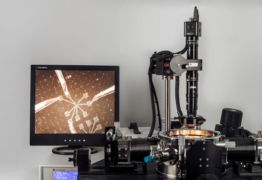
SPM (scanning probes microscope) represent the basis for modern scientific research laboratories. Their primary objective is the measurement of the topographic surface properties, from which a picture of the sample can be obtained.
We can scan both conductive (with STM – scanning tunneling microscope) and insulating samples (with AFM – atomic force microscope). The basic idea lies on the atomic interaction between the sharp scanning tip and the atoms on the surface. This allows us to get atomic scanning resolution, which opens a variety of possibilities for the research of new nanomaterials.
The tip can also be used as a manipulator for small particles, at low temperatures even for a single atom. This device thus represents the basis for the nanotechnology for it enables us to perform experiments on atomic level, which were until now impossible.
Responsible person:
Petra Šutar
Tel: + 386 1 477 3437
petra.sutar@ijs.si
Location:
Jožef Stefan Institute
Department of Complex Matter
Room C 104
Jamova cesta 39
SI-1000 Ljubljana, Slovenia
